How do games work?
Okay…. This isn’t a definitive guide to how every game works, its just a guide to how the pieces on SOME boards fit together. Understanding how a computer system works brings you much closer to being able to understand how to troubleshoot problem boards. Its no good getting an oscilloscope or logic probe if you don’t know how to interpret the results you get.
Now I’m not an expert, I’m just a collector - but I once was a Z80 programmer and knew a fair bit about how the system works. Obviously you don’t need to know how a car works to drive one, but with writing assembly language (machine code) you need to know a little about the system to understand how the instructions work. Now, I’m not going to jump off the subject matter here, this is just a short introduction to:
How a computer system works
This is based on the Z80A computer the Sinclair ZX Spectrum, but its theories can be applied to most other processors. Obviously, things like pinouts are different from processor to processor, but how it works remains (mostly!) the same. My computer studies teacher taught us that a computer is a machine that obeys instructions, nothing more nothing less. Lets take a look at the actual diagram I was given:
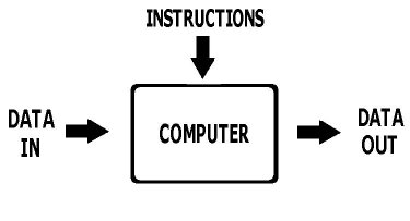
Now I dunno if it was just me, but I didn’t really find that particularly helpful! I suppose it is really, but it wasn’t until a lot later on that we were given this:
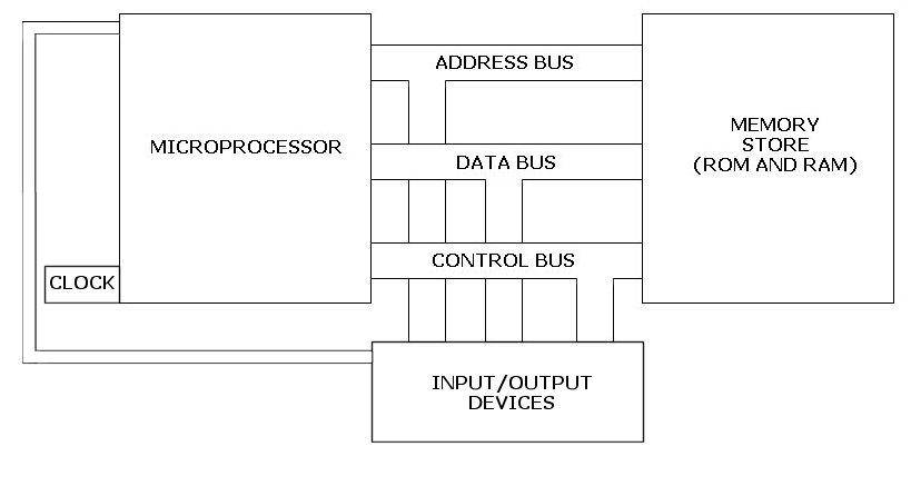
Now here’s a little information about what’s going on here… This may be geared towards an actual computer, but arcade boards are just the same. This description does skip the need for complex video and sound circuitry in favour of understanding more about the processor (who knows I may even add more about video and sound later on!) Okay this diagram shows the general arrangement used in a Z80 computer. Right… This is a little simplistic but I’ll explain in greater detail a bit later, for now just trust me on this! As you can see the processor is the main part of the system, it is the part that takes the program and turns the code into output using your input to determine what happens. Code is stored in ‘pigeon-holes’ in the ROM/RAM, diagrams are a far better way to explain it:
Memory Address:    Code:
    32768:          062
    32769:          001
    32770:          061
Now obviously this is a very short program! But its to demonstrate how code is executed. The instructions are carried out sequentially, the processor holds the current memory address in the program counter which is (simply) the address bus. The data bus is used to transfer data between the processor and the memory. The data bus is bi-directional, meaning that it is used by the processor to take data and instructions from memory AND to place data into memory. There aren’t separate input and output buses on a processor, the data bus does both jobs. The control bus makes sure that all elements of the system are operating together in unison, if the processor sends data to a register the control bus makes sure that it is ready to receive it. ROM stands for - READ ONLY MEMORY and is the type of memory that holds the game (or whatever) code, RAM stands for RANDOM ACCESS MEMORY and is the type of memory that holds temporary data, such as high scores or even the games display screen/graphics. Now back to that little program, although this looks like a load of numbers the processor knows what to do with them. It makes it a whole lot easier to understand to you and me though if we convert the code to mnemonics (like BASIC keywords) therefore the program we have does this:
062, 001 :  LD A, 001   ;LoaD the A register with 001
061      :  DEC A       ;DECrease A by 1 (making it zero!)
So you see, not a very useful program!!! As you can see 062 stands for LD A,??? and 061 for DEC A, I didn’t want to stray too far into this only really to show how the processor and buses work.
Here is a Z80 pinout:
Right! Now we’re getting somewhere! The address bus is shown here by A0-A15.
Here’s another technical bit… The Z80 deals with bytes which are one ‘piece’
of data each byte is made from 8 bits which are either 0 or 1 (on or off) the
maximum number it can hold if ALL bits are on is 256 therefore addresses which
are obviously much larger numbers than 256, are made from TWO bytes together
making 16 bits, 256 X 256 = 65536 or exactly 64K of memory. Larger systems have
’extra’ memory arranged in pages, which can be toggled by the programmer to
replace the existing memory page (without erasing it I might add!) For the
purposes of arcade boards, bits are on or off - which for testing purposes
means ON=+5v OFF=0v, bear in mind that A0-A15 is 16 bits counting 0 itself as
one! The data bus is D0-D7 (8 bits) and lastly, the control bus which is 13
different signals (and is of more interest with regards to repair). There are 8
outputs and 5 inputs, the first of these is:
RD (imagine the line is above NOT below, unfortunately HTML doesn’t allow for
this…) which is MEMORY READ. This indicates the CPU wants to read data from a
memory location or input/output port. The signal is active low and is present
whilst the address bus holds a valid address. RD is used by the addressed
location or port to gate data onto the data bus. WR which is WRITE, indicates
that the CPU requires to send data to a store location or input/output port.
The signal is also active low and is present whilst the address bus holds a
valid address and the data bus valid data. WR and RD are effectively strobe
signals, meaning they indicate when it is okay to read/write when everything is
valid (different processors use slightly different signals).
MREQ is MEMORY REQUEST, is an active low signal indicating that the address bus
holds a valid address. It appears in conjunction with RD or WR remember one is
READ one is WRITE…
IORQ is INPUT/OUTPUT REQUEST. An active low signal indicating that the address
on the first byte of the address bus (A0-A7) is the address of an input/output
port and that a transfer is to be performed. IORQ allows memory locations and
I/O ports to share the same address. It appears with RD and WR to indicate if
data is input or output. It is also used with the timing of interrupts, which
I’ll cover later…
RFSH is REFRESH an active low signal indicating that A0-A6 contain an address
that can be used to refresh dynamic memories (such as a 4116). The data is
stored as charges on capacitors which have to be refreshed every few
milliseconds. Unlike other processors the Z80 has its own refresh logic (others
need external logic to gain control at regular intervals to perform the refresh
operation) anyway, the refresh address is placed on the lower 7 bits of the
address bus along with a refresh signal on RFSH (the control bus) when the bus
is free. MREQ appears with RFSH.
HALT indicates that the processor has halted after a HALT instruction (the
signal is active low). The memory refresh for dynamic memories continues even
though the processor is halted though.
M1 is machine cycle one. There are three things that need to be done to execute
an instruction, it needs to be fetched from the data store (M1) followed by a
memory read (M2) and/or a memory write (M3). M1 goes active low when the
processor is in the M1 ‘fetch’ state. The signal is used for timing.
WAIT is used for timing too, when the signal goes active low the processor
simply waits… This is because the processor may be faster than some of the
components its using, therefore it needs to know when the required data
transfer can take place. During a WAIT state the memory refresh is NOT
maintained.
RESET is used to force the processor into a known state by resetting itself.
The program counter/interrupts/refresh are all reset to zero (interrupts are
disabled). This is used at power on or to regain control if a program crashes.
You will notice the signal is active low then held high on power on, the active
low is the reset when power is turned on and the high is normal operation. A
circuit called the watchdog circuit or watchdog timer is connected to RESET it
receives a signal from the code which resets a countdown, if the code crashes
and the countdown finishes the watchdog will reset the processor.
INT and NMI are interrupts and non maskable interrupts. Interrupts allow a
device requiring attention to signal directly to the processor that it needs to
execute some ‘servicing’ code. Interrupts have low->high priorities and can be
ignored by the processor, on the other hand a non maskable interrupt can’t be
ignored.
BUSRQ is BUS REQUEST and is an input from a device requesting control of buses.
When the signal is active low the processor sets all its bus signals to a high
impedance state, it then takes BUSAK (BUS ACKNOWLEDGE) active low to allow the
requesting device to take control. When the buses are released from the
processor, memory refresh is NOT maintained.
The only other connections are VCC which is the main input voltage (+5v), 0v or GND which is ground for the power supply and CLK or 0 which is the clock signal (a crystal oscillator which supplies 1, 2 or 4MHz depending on which processor you’re using).
But What About Arcade Games?
Right now you understand how the system works lets look at arcade boards… Now remember this doesn’t apply to EVERY board you may own… There is a ‘block’ of memory assigned for the screen and when code is written to it, things appear there. There are variations on this such as Pacman, where the game puts a number corresponding to a game character into a different block of memory and then a separate program which is called by an interrupt reads this block and then refreshes the screen memory with the updated characters (using graphics rather than the code) this is greatly simplified, as there are then separate circuits for moving the character sprite pixel by pixel using the rotate commands on the Z80, but that’s a little too involved for this guide.
UNFINSHED!!!!